ZYNQ防火墙开发9-PS-PL通信-AXI-DDR

PS和PL通信机制

image-20240323150812473

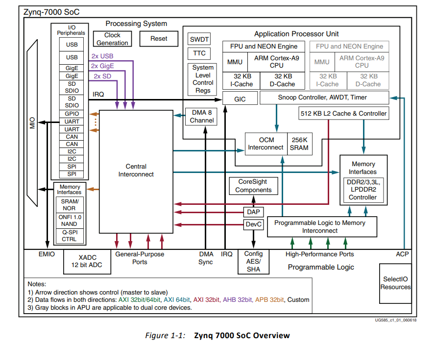
​ 所有 Zynq-7000 AP芯片上的存储器接口单元包括一个动态存储器控制器和几个 静态存储器接口模块。动态存储器控制器可以用于 DDR3、DDR3L、DDR2 和 LPDDR2。 静态存储器控制器支持一个 NAND 闪存接口、一个 Quad-SPI 闪存接口、一个并行数 据总线和并行 NOR 闪存接口 [9]。

Screenshot_20240424_140715

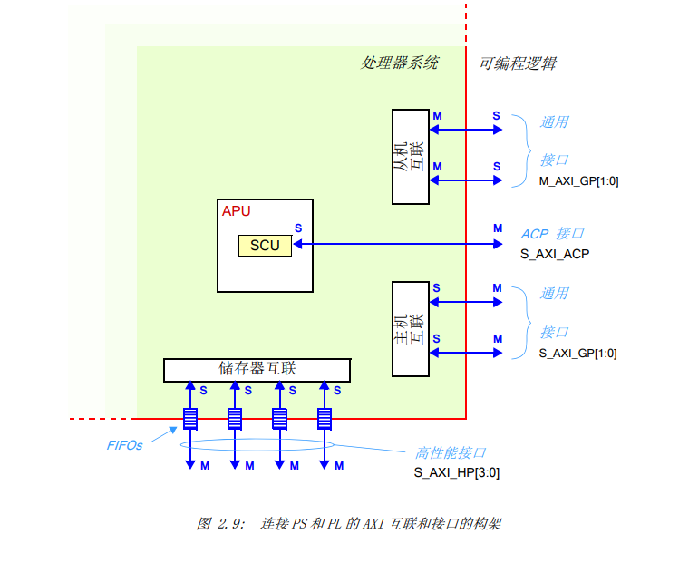
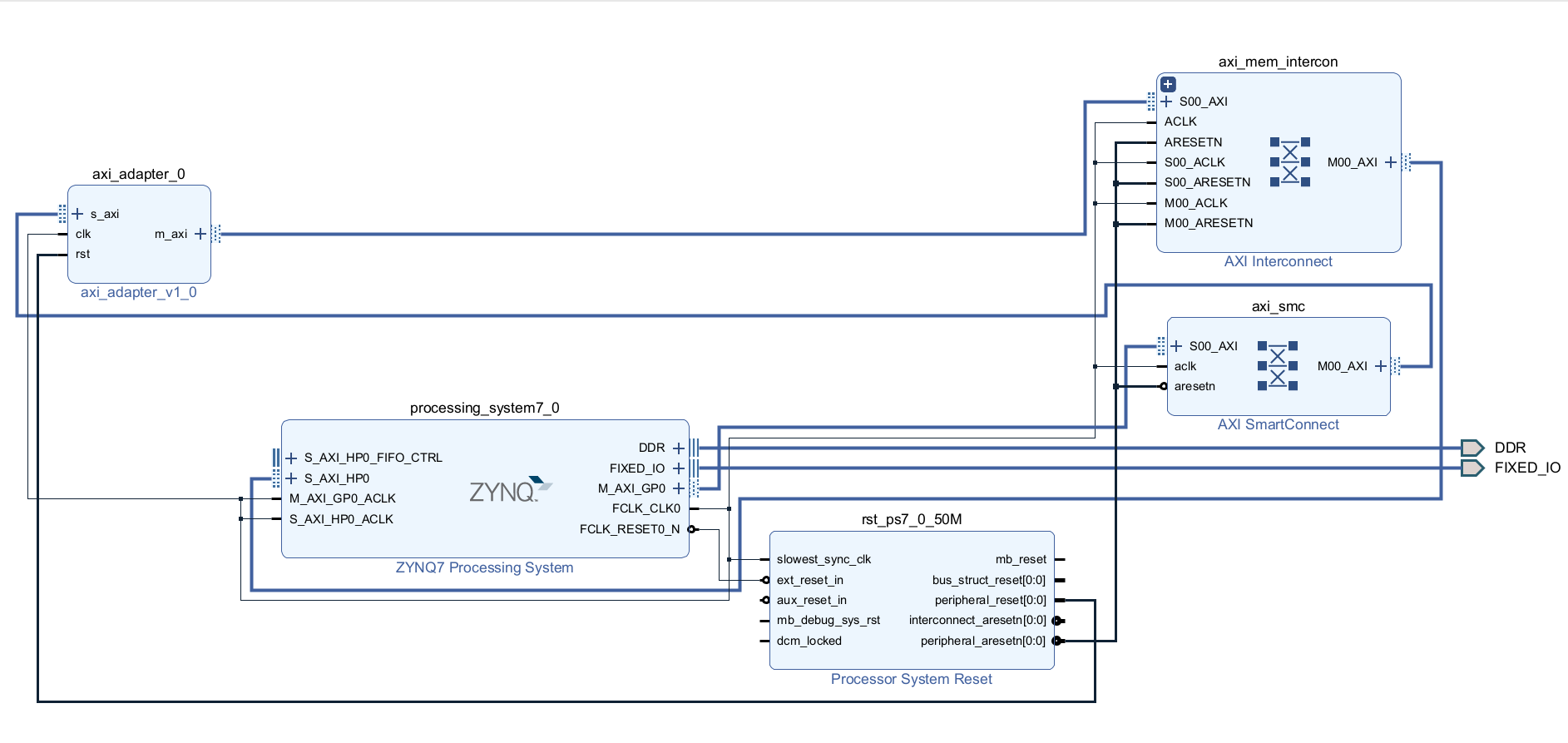
​ 之前课程我们用到的都是GP接口,这节课开始使用HP接口进行访问。通过上图可以知道HP是直接连接到存储控制器上的,然后再连接到DDR。由于PS侧是DDR,所以对于AXI,PL侧的HP接口都是Master。

image-20240917122258095

地址空间

OCM

The on-chip memory (OCM) module contains 256 KB of RAM and 128 KB of ROM (BootROM). It supports two 64-bit AXI slave interface ports, one dedicated for CPU/ACP access via the APU snoop control unit (SCU), and the other shared by all other bus masters within the processing system (PS) and programmable logic (PL). The BootROM memory is used exclusively by the boot process and is not visible to the user.
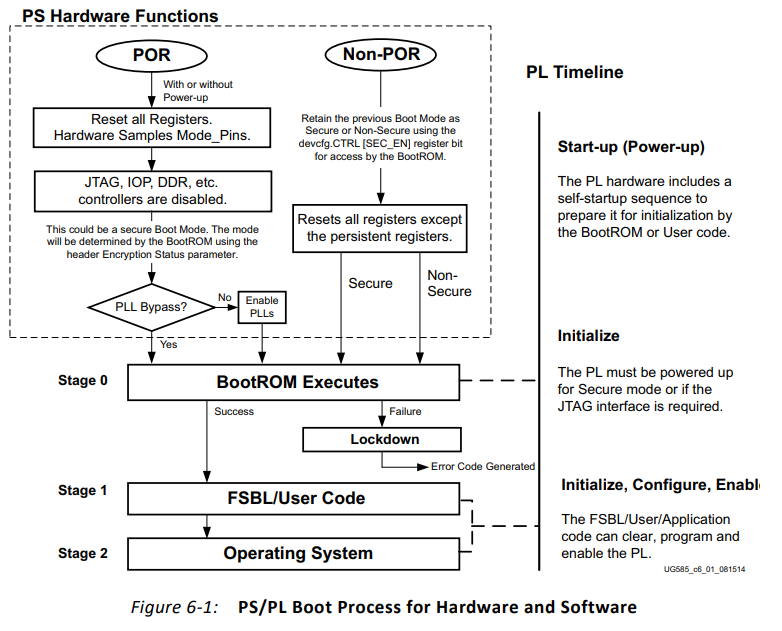
zynq启动流程

​ 动态存储器接口 这个多协议双数据速率 (Double Data Rate,DDR)存储器控制器包括三个主 要的模块:一个核心存储器控制器和调度器 (DDRC) 、一个 AXI 存储器端口接口 (DDRI)和一个数字 PHY 以及控制器 (DDRP)[3]。

​ DDR 存储器控制器可以被配置为 16 位或 32 位模式,能在配置为 8、16 或 32 位 的单个块的 DRAM 存储器中访问 1GB 地址空间。也支持 EEC 存储器,但是只能以 32 位模式访问。用 DDR3 的时候支持最大 1333Mb/s 的速度 [9]。 对 PS 和 PL 的共享存储器的共享访问是通过多端口 DDRI 来支持的,它具有四个 AXI 从机端口来满足这个要求 [9]: • PL 通过两个专用的 64 位端口 (AXI_HP)来访问。 • 一个 64 位端口通过 L2 cache 控制器专用于 ARM CPU。这个端口可以被配置为 低延迟。 • 所有其他 AXI 主机通过中央互联共享剩下的端口。 每个 AXI 接口配备有专用的事务 FIFO。

​ DDRP PHY 处理从控制器来的读 / 写请求,并在 DDR 存储器的时序约束下,把请 求翻译为信号。PHY 用控制器来的信号创建内部信号,通过数字 PHY 传递到 DDR 引 脚上。最后通过 PCB 上的走线把 DDR 引脚接到实际的 DDR 芯片上。

图 10.3 是 DDR 存储器控制器的框图 Screenshot_20240408_161415

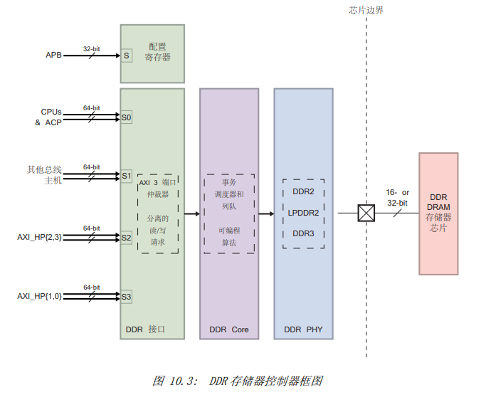
​ 将寄存器AXI TARGET SLAVE BASE ADDR的值修改为0x8000000,这个地址将作为我们PL对DDR进行读写的起始地址,这里有个值得注意的地方,用0x8000000而不是0x00000000 是因为0x00000000这个地址属于OCM 片内存储器的, 又因为DDR的前面部分地址需要给程序堆栈使用,所以这里我们才选地址为0x8000000。

​ 对于 DDR 存储器控制器的深入信息,请参考 《Zynq-7000 All Programmable SoC Technical Reference Manual》的第 10 章 [3]。

DDR初始化大致分为2个步骤

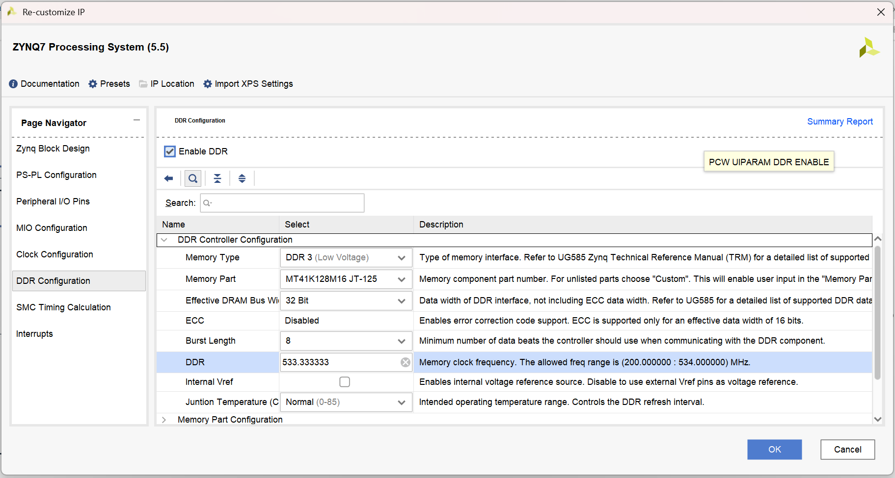
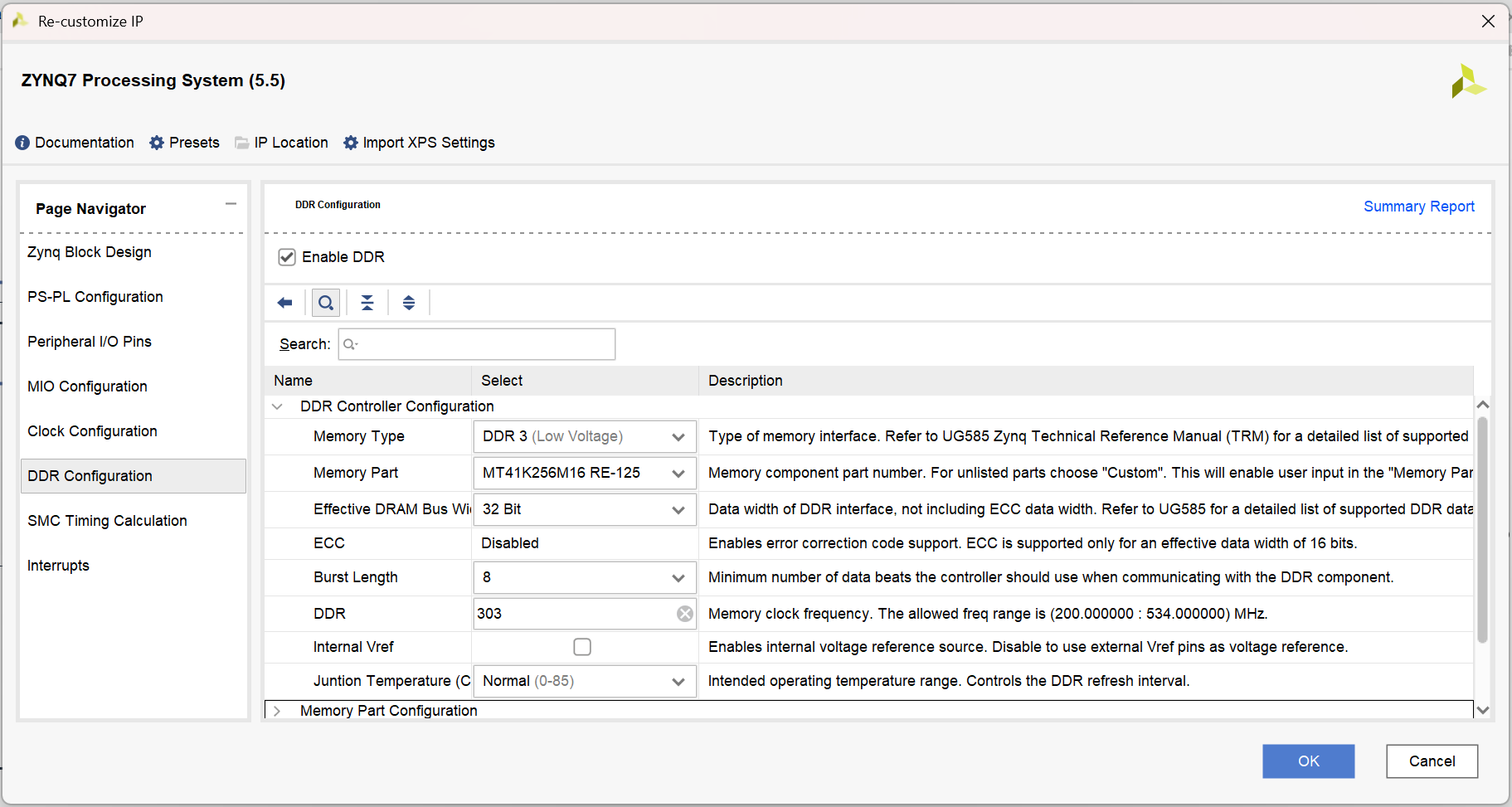
1、在Vavido中配置好DDR型号,位宽等。生成ps_init.c初始化文件。

2、在Board.c(u-boot-xlnx-xilinx-v2014.4\board\xilinx\zynq)路径下的dram_init函数中。设置dram大小。

​ 有2种方式设置 (1、可以从设备树中获取,通过打开CONFIG_OF_CONTROL宏 2、可以通过代码中写死的宏定义CONFIG_SYS_SDRAM_SIZE(zynq_zed.c)来修改。)。

fsbl_hwproj

1
2
3
4
5
6
7
8
9
10
11
12
13
14
15
16
17
18
19
20
21
22
ps7_init() 
{
// MIO init
ret = ps7_config (ps7_mio_init_data);
if (ret != PS7_INIT_SUCCESS) return ret;

// PLL init
ret = ps7_config (ps7_pll_init_data);
if (ret != PS7_INIT_SUCCESS) return ret;

// Clock init
ret = ps7_config (ps7_clock_init_data);
if (ret != PS7_INIT_SUCCESS) return ret;

// DDR init
ret = ps7_config (ps7_ddr_init_data);
if (ret != PS7_INIT_SUCCESS) return ret;

// Peripherals init
ret = ps7_config (ps7_peripherals_init_data);
if (ret != PS7_INIT_SUCCESS) return ret;
}

​ Ps7_init.c和ps7_init.h,用于初始化CLK,DDR和MIO。Ps7_init.tcl完成的初始化和ps7_init.c代码完成的初始化是相同的。

​ Ps7_init.tcl文件,可以用来初始化CLK,DDR和MIO。它所完成的初始化和ps7_init.c代码完成的初始化是相同的。

​ 注意:当使用XMD调试应用程序的时候tcl文件是很有用的。例如,你可以执行Ps7_init.tcl文件然后将应用程序加载到DDR中并调试。在这种情况下,就不需要进行FSBL的全过程。

1
2
3
4
5
6
7
Following operations will be performed before launching the debugger.
1. Resets entire system. Clears the FPGA fabric (PL).
2. Program FPGA fabric (PL).
3. Runs ps7_init to initialize PS.
4. Runs ps7_post_config. Enables level shifters from PL to PS. (Recommended to use this option only after system reset or board power ON).
5. All processors in the system will be suspended, and Applications will be downloaded to the following processors as specified in the Applications tab.
1) ps7_cortexa9_0 (/home/dnsnat/workspace/database/source/fpga_project/ZYNQ/gateway_src/PS_AXI_DDR/PS_AXI_DDR.sdk/PS_AXI_DDR/Debug/PS_AXI_DDR.elf)

Initialize the PS

1
2
3
4
5
6
1. Load ps7_init. tcl using the commandsource ps7_init. ...
2. Use the “connect” command to connect to the Zedboard.
3. Use the “targets” command to get a list of targets (you could skip this).
4. Use the command “target 1to select your target.
5. Call “ps_init” and then “ps_post_config”.
6. The PS is now initialized.

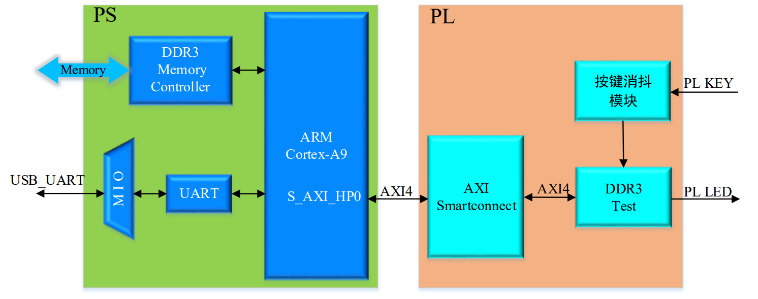
AXI-DDR工程和上一节AXI-RAM相似,附件包含了AXI_DRR_IP核,

image-20240919105239482

EBAZ4205开发板配置

image-20240919105731729

sdr开发板配置

image-20240919105426227

以下为vtis代码:

1
2
3
4
5
6
7
8
9
10
11
12
13
14
15
16
17
18
19
20
21
22
23
24
25
26
27
28
29
30
31
32
33
34
35
36
#include <stdio.h>
#include "platform.h"
#include "xil_printf.h"
#include "xparameters.h"
#include <xil_io.h>
#include <sleep.h>

#define PhyRead(addr) Xil_In32(addr)
#define PhyWrite(addr, value) Xil_Out32(addr, value)
#define AXILITE_BASEADDR XPAR_AXI_ADAPTER_0_BASEADDR + 0x8000000

int main()
{
init_platform();

print("Hello World\n\r");
for(int i=0;i<3;i++)
{
sleep(1);
printf("i is %d\n\r",i);
}
int reg0in = 320;
int reg0out = 0;

//可以通过debug模式查看memory,对比没有disable的情况
Xil_DCacheDisable();
for(int i = 0; i < 32; i+=4)
{
reg0out = PhyRead(AXILITE_BASEADDR + i);
PhyWrite(AXILITE_BASEADDR + i, reg0out + 4);
printf("reg0out %x is %d\r\n", AXILITE_BASEADDR + i, reg0out + 4);
}

cleanup_platform();
return 0;
}

附件:

axi_adapter.rar


ZYNQ防火墙开发9-PS-PL通信-AXI-DDR
http://witbit.cn/视频课程/FIREWALL_GATEWAY/ZYNQ防火墙开发9-PS-PL通信-AXI-DDR.html
作者
朝彻
发布于
2025年2月13日
许可协议